Manipulation and coherent Control of Phonons PHONUIT: Phononic Circuits
The understanding and ability to manipulate phonons as quantum particles in solids enable the control of coherent phonon transport, which is of fundamental interest and could also be exploited in applications. Logic operations can be realized with the manipulation of phonons both in their coherent and incoherent form in order to switch, amplify, route signals and to store information. If brought to a mature level, phononic devices can become
complementary to the conventional electronic ones, opening new opportunities.
With PHONUIT, we tackle the challenges of nanophononics both from the materials point of view, i.e. engineering the phononic properties of nanostructures, as well as from the methodology point of view, i.e. pushing the limits of currently existing experimental methods and developing novel measurements methods and platforms. Specifically, this project aims to realize a phononic integrated circuit, where phonons in coherent and/or incoherent form are generated, routed and detected on chip.
For the realization of integrated phononic circuit, we have worked in parallel on the different aspects that are needed for their design and development:
1. Enhancement of existing Methods & Development of novel Methods
We investigate the phononic properties of nanomaterials with either inelastic light scattering spectroscopy, ultrafast techniques, or with thermal conductivity measurements.
- Space- and time-resolved spontaneous/stimulated Raman Spectroscopy and coherent anti-Stokes Raman
- Space- and time-resolved hot spot relaxation measurements
- Novel measurement platforms for thermal transport
- Novel method for single nanostructure absorption measurements
2. Phonon Engineering
In order to excite phonons with desired frequencies, we need to engineer the phononic properties of materials. Nanowires (NWs) offer the unique possibility to controllably obtain novel semiconductor materials in terms of crystal phase. This enables the fine tuning of their phononic, optical and electronic properties.
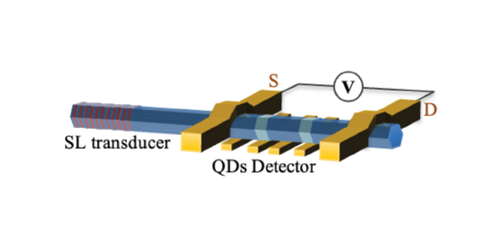
Furthermore, we want to tailor the phonon spectrum by means of nanostructuring combined with heterostructuring (i.e. the combination of different materials with different elastic properties). In particular, we envision the implementation of superlattices (SLs) into NWs, switching periodically the material and/or the crystal phase.
3. Thermal Circuits Elements
- Phonon sources and detectors
We came up with an innovative idea to launch and detect phonons with quantum dots (QDs). The semiconductor double QDs support zero-dimensional electronic states and the electron tunnelling is driven by a finite source drain bias. Single-electron tunnelling events through two QDs coupled in series can be accompanied either by emission (absorption) of a photon and a phonon. Under specific conditions, phonon emission (absorption) greatly dominates over photon emission (absorption). We have achieved the realization of this device concept with in-built InP barriers in InAs nanowires and we could recently reach the weakly coupled regime of the double QD defined in the three barrier NW. - Thermal diode
A thermal diode is a device which allows heat transport when a forward thermal bias is applied, behaving as a thermal conductor, and inhibits thermal transport for reverse thermal bias, behaving as a thermal insulator. This project aims at investigating the thermal rectification characteristics of telescopic and heterostructured nanowires using the suspended platforms for thermal conductivity measurements in combination with spatially resolved Raman thermometry.
Publications
Team Members
Former Team Members
Funding

This project has received funding from the European Research Council (ERC) under the European Union’s Horizon 2020 research and innovation programme (Grant agreement No. 756365)


