Thesis_Grazia
Grazia Raciti (2020-2025)

Probing Dynamic Processes in Semiconductor Materials Using Ultrafast Spectroscopy

In this thesis, we develop a multi-technique pump-probe setup capable of performing both transient reflectivity (TR) and time-resolved Raman spectroscopy (TRRS), monitoring changes in reflectivity or Raman spectra, respectively, after ultrafast excitation. We demonstrate that combining these two techniques provides a comprehensive understanding of ultrafast electronic and phononic processes. We use TRRS and TR to study bulk semiconductors such as silicon (Si) and germanium (Ge). We used the investigations on Si to benchmark the setup, while our measurements on Ge reveal new and interesting physics. We observe distinct decay rates for the temperature, frequency, and linewidth of the phonon mode in Ge, along with the propagation of coherent acoustic phonon oscillations.

Our approach is extended to Ge/SiGe heterostructures and 2D materials, demonstrating the validity of our techniques also in nanostructures and low-dimensional systems. We were able to decouple the relaxation dynamiics of a quantum well as thin as 15 nm from that of the SiGe barrier layer, as well as to probe Brillouin oscillations in the system. Furthermore, CVD multilayer graphene samples were investigated using both frequency-domain thermoreflectance and beam-offset frequency-domain thermoreflectance. The latter is a technique developed at the Institut de Ciència de Materials de Barcelona, in the group of Dr. Sebastian Reparaz, to explore in-plane thermal diffusivity. While spending a research stay in the group of Dr. Reparaz, we contributed to the validation of the method, and we exposed the different thermal response of multilayer graphene, depending on the number of layers.

Thesis Arianna
Arianna Nigro (2021-2025)

Development of planar Ge/Si_(1−x)Ge_x heterostructures for quantum computing

In the first part of this thesis, we presented a detailed study on the growth kinetics, morphology, and crystal quality of Ge thin films grown via chemical vapor deposition, examining the effects of growth temperature, partial pressure of the precursor gas, and the use of Ar or H2 as carrier gases. We observed that the presence of a carrier gas enhances the deposition rate and promotes surface smoothening in Ge films grown at low temperatures. The surface roughness, crystalline quality, and defect density of the films were analyzed across the explored deposition conditions, revealing the formation of crystalline structures under all conditions, with lower defect densities at higher deposition temperatures.

In the second part of this thesis, we present the development of optimized growth conditions for each constituent layers of the heterostructure. Ge virtual substrates were deposited using a two-step temperature approach, involving the initial deposition of a thin layer at low temperature
followed by the regrowth of a thicker layer at a higher temperature to ensure smooth surfaces. We carefully controlled the chemical composition of the Si1–xGex graded layer and the Si1–xGex barriers by adjusting the flow rates of the GeH4 and SiH4 precursor gases. Epitaxial growth of the Ge quantum well was achieved with precise control over layer thickness. Growth conditions were engineered to produce atomically sharp transition regions between the Ge quantum well and the two Si1–xGex barriers. Furthermore, we present preliminary studies on the controlled oxidation within the reactor chamber of the protective Si cap terminating the structure.

Finally, we exploited the degrees of freedom of the layout to assess their influence on the structural and electronic properties of the heterostructure and device performance for quantum applications. The strain level in the Ge quantum well was systematically tuned by modifying either the well thickness or the chemical composition of the Si1–xGex barriers, resulting in compressive strain in the in-plane direction, and tensile strain in the out-of-plane direction. The strain-induced energy splitting between the heavy hole and light hole bands was experimentally measured, confirming that the implemented layout energetically favors the former. Devices exhibiting promising transport and photon coupling properties were realized, demonstrating the compatibility of our structures as building-blocks for hybrid quantum devices.

Thesis Nadine
Nadine Denise (2019-2025)

Quantum structures in GaAsN nanowires and quantum wells: Physical properties on-demand by hydrogen implantation

Thesis Nicolas
Nicolas Forrer (2020-2024)

Germanium/Silicon Nanowire Heterostructures for Quantum Computing

In the first part of this work, a detailed study on the growth kinetics of silicon and germanium nanowires, employing the vapour-liquid-solid growth method catalysed by gold, is presented. The effects of temperature, partial pressure, and carrier gas for different precursor gases on the nanowires’ growth kinetics and structural properties are evaluated by means of scanning electron microscopy. Here, it was found that argon as carrier gas enhances the growth rate at higher temperatures, while hydrogen does so at lower temperatures, due to the lower heat flux. For both precursor gases two growth regimes as a function of temperature were found. The tapering rate of the silicon nanowires is about an order of magnitude lower than the one of germanium nanowires. Furthermore, optimal conditions for NWs nucleation have been identified for both materials. Different catalyst deposition techniques have been investigated, namely electron beam lithography and colloidal deposition. Here, the colloidal deposition shows high ease of usage and high control over the size, while lacking the freedom of choosing different materials or a precise control over position and density. This freedom is given by the lithography approach, though its optimisation requires more effort. In the pre-growth preparation, hydrofluoric acid is often employed to enable epitaxial growth. Different hydrofluoric acid concentrations have been tested to find an optimal one around 2%. Germanium buffered substrates are a way to reduce the usage of hydrofluoric acid, making the process safer.

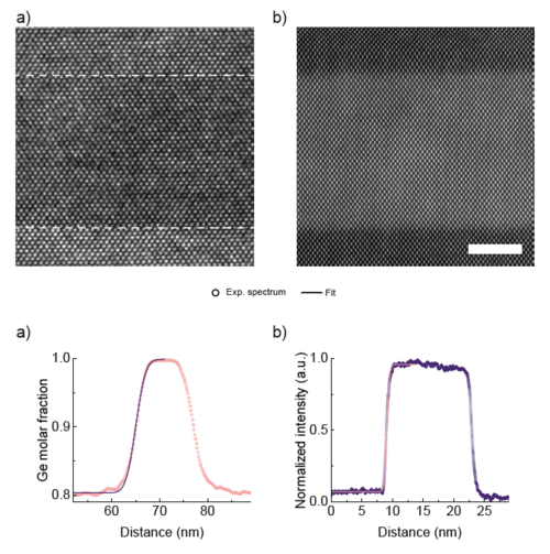
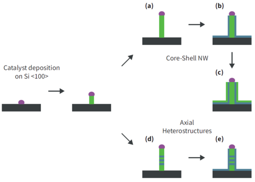
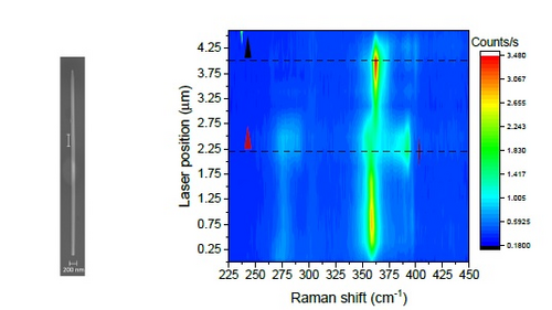
In the second part germanium-silicon core-shell nanowires were grown employing chemical vapour deposition techniques. Thereby, a two-step growth procedure for the growth of germanium core is introduced and optimised for optimal crystal quality and low tapering rates. An optimal temperature of 350 °C for nucleation and a lower temperature of 280 °C for the elongation of the wires has been found. The change of temperature worked best for growth total pressure of 1Torr and 2Torr, while the gas mixture used during the whole growth is germane 10% in argon. Approaches have been tested to deposit thermal silicon shells. Several recipes were tried, most of them leading to no shell growth. Therefore, efforts have been made to deposit the silicon shell at low temperature (250 °C) by a plasma enhanced reaction. This lead to high control over the thickness of a crystalline silicon shell, with a growth rate of about 1.8nmmin−1. Raman measurements of germanium-silicon core-shell nanowires revealed a compressive strain in the germanium core, which increases with increasing shell thickness. Furthermore, high resolution transmission electron microscopy proved the crystal direction to be ⟨110⟩ and (poly- or single) crystallinity.

Other germanium-silicon heterostructures were grown, namely curved germanium quantum wells and axial silicon barriers. Two growth procedures for curved germanium quantum wells have been tested and optimised, one employing the plasma, the other thermal deposition. It was observed that with the plasma enhanced deposition the pressure influences the growth rate of the shell much more than the plasma power. Thermal shell deposition of germanium was also reached, leading to symmetric and homogeneous shells. First experiments on axial silicon barriers have been conducted. It was found that the transition from germanium to silicon works very well, while the reversed transition is more challenging due to the different saturation levels of silicon and germanium in gold.

Thesis_Yashpreet
Yashpreet Kaur (2019-2023)

Thermal rectification in designed nanowires

This dissertation recites an experimental study in search of a solid-state system for applications in thermal circuit elements, specifically a thermal diode. For this purpose, we studied a quasi-1D nanostructure referred to as telescopic nanowires. These structures are notably interesting since they have two segments with a thick and a thin part with a transition region in between along the growth axis. Due to their special structure, the temperature dependence of thermal conductivity could be used as a mechanism to inspect thermal rectification.

To study telescopic nanowires, electro-thermal and opto-thermal techniques were employed. For this purpose, well-known thermal bridge devices were fabricated to study heat transport in small samples. The experimental investigation was carried out by transferring nanowires through micro-manipulation on the thermal bridge devices. To do so, thermal bias was applied in forward and reverse bias conditions by joule heating the suspended platforms, which acted as heaters as well as thermometers. As a result, thermal conductance values were extracted. In particular, the thermal conductance values were found to be higher when the heat flow was in the direction of thick to the thin part as compared to thin to thick direction. The asymmetric heat flux is a signature of the thermal diode. Therefore, we were able to estimate thermal rectification in telescopic nanowires. The direction of rectification was attributed to the effect of thermal boundary resistance between the thick and thin parts of the nanowire. Using the opto-thermal method of Raman thermometry, the impact of thermal contact resistance was predicted and estimated by developing an equivalent thermal circuit model for our experimental system.

Image Diego Thesis
Diego de Matteis (2018-2023)

Phonon engineering in nanowire heterostructures

The work presented in this thesis falls in the field of Nanophononics. The majority of the thesis describes our investigation of heat carrier dynamics in several novel nanostructured semiconducting materials, namely core-shell hexagonal phase GaAs – SixGe1-x (0 ≤ x ≤ 0.59) nanowires, and nanowires containing GaAs-GaP and InAs-InP superlattices (SLs). For the core-shell nanowires, we assess the good crystalline quality of the samples, probe the energy and symmetry of electronic transitions through their coupling with phonons, highlight the effect of a novel kind of stacking fault on the Raman spectra and analyse the complex alloy lattice dynamics, while quantifying the effects of chemistry- and geometry- induced disorder. For the SL nanowires, we investigate several SL periods and architectures, unveiling the tailorability of the phonon spectrum, the emergence of Surface Optical phonon modes in the InAs-InP system, and the high quality of the heterostructures. A second set of efforts described in the thesis is directed at the long-term goal of creating purely phononic devices, i.e. circuits where information and/or energy is transported by phonons, like current does in electric circuits. We worked, both in the design and implementation phase, towards creating a versatile experimental setup, allowing for multiple experiments, all based on pulsed laser beams. These techniques allow, for example, to follow global lattice dynamics with high time resolution or to excite and then monitor in time and space the dynamics of a specific phonon mode with a defined energy and symmetry. This is crucial information for the realization of phononic devices and for the integration of phonon-based functionalities in other technologies. The materials and the structures investigated in this thesis are the result of cutting-edge synthesis processes that represent, in the case of hexagonal phase SixGe1-x, a long-sought after goal in optoelectronics and in the case of the SLs a remarkable degree of control in fabricating nanostructures with on-demand properties. Therefore, as the evidence illustrated in this thesis constitutes a step towards a better understanding of nanoscale phononics, we believe we can inform the design of ever more energy-efficient devices, capable of harnessing the potential of heat.

Thesis_Medina
Medina Umar (2016-2020)

Deposition and Characterization of Wide Band Gap P-Type Metal Oxides for Photovoltaic Applications

In this work, we perform deposition and characterization of thin films of copper oxides to be used in photovoltaic devices. Thin films of copper oxide were grown by radio frequency-magnetron sputtering in an oxygen-argon environment onto silicon and FTO-coated substrates at two different oxygen partial pressures (15% and 23%). Control over the oxygen flow during deposition is of paramount importance and quite difficult, making reproducible growth challenging. Post deposition annealing in vacuum environment was conducted on the films at different temperatures (between 250°C and 550°C), as an alternative pathway towards the creation of the desired phase and stoichiometry of copper oxide films in a reproducible manner.

We investigated the surface morphology of the thin films by Scanning Electron Microscopy, Energy Dispersive X-ray, Atomic Force Microscopy and Kelvin Probe Force Microscopy. These studies show that the pristine films are made up of densely packed grains that are homogeneously distributed. In the annealed thin films, the size of the grains evolves greatly with the annealing temperature increase: besides the change in the morphology of the grains, which become bigger and less homogeneous, the films become nano porous in the annealed samples. The contact potential difference measurements show the presence of some islands in samples annealed at temperature higher than 450°C, only above this temperature, that the regions with higher and lower CPD values correlated with higher and lower work functions, respectively. Suspecting that these areas represent the co-existence of CuO and Cu2O crystals.

The structural properties of the thin films were studied via spectroscopy and X-ray diffraction and Raman, which reveal that two oxide phases (i.e. CuO and Cu2O) co-exist in the films deposited with high oxygen ratio. In particular, high oxygen pressure during deposition favours CuO and annealing in vacuum converts CuO to Cu2O. Instead, low oxygen pressure directly promotes the formation of Cu2O thin films. In the thin films deposited on glass, we also performed transmission measurements and found that the transmittance of films is higher in the near IR region while absorption is higher at the ultraviolet to visible region of the spectra.

Finally, we uncovered a novel parasitic crystallite growth as a result of aging on the pristine and low-temperature annealed samples, and we found out that high temperature annealing prevents this kind of aging. This aging effect is completely absent in the thin films deposited onto the FTO substrates.

Nach oben